
 OpenMV MicroPython
Arduino Giga R1 WiFi
The Arduino Giga R1 WiFi is a 101 × 53 mm Mega‑form‑factor board built around the STMicroelectronics STM32H747XI — a dual‑core SoC combining a Cortex‑M7 at 480 MHz with a Cortex‑M4 at 240 MHz. The OpenMV firmware runs entirely on the M7 core. The Giga adds a 22‑pin Arducam camera flex connector, a MIPI‑DSI connector for the Arduino Giga Display Shield, and a 3.5 mm stereo audio jack to the standard Arduino Mega header layout.
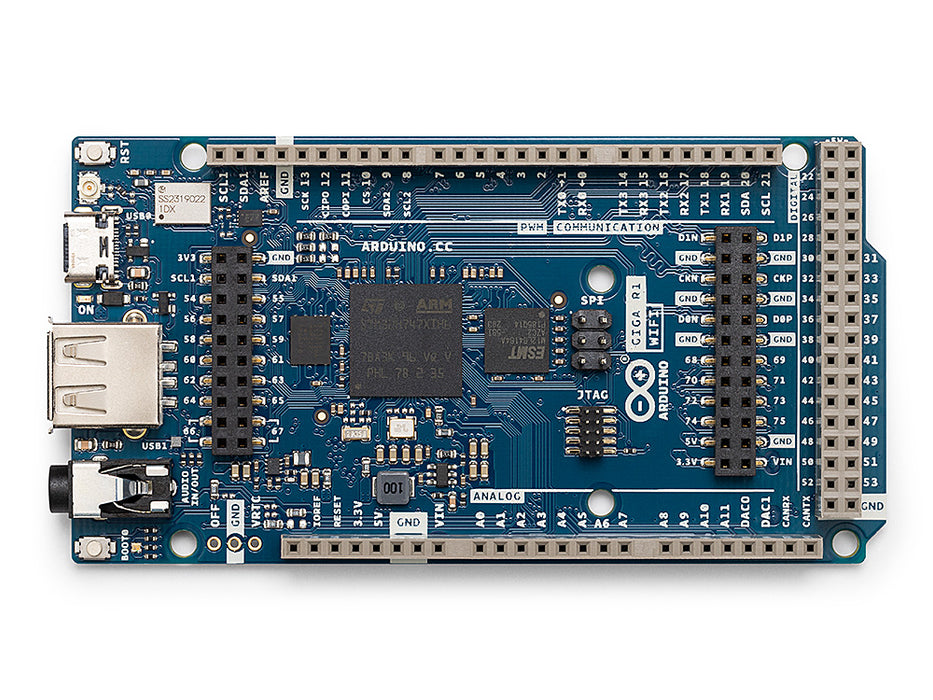
For full datasheet, photos, and dimensions see the Arduino Giga R1 WiFi product page.
Highlights
STMicroelectronics STM32H747XI dual Cortex‑M7 (480 MHz) + Cortex‑M4 (240 MHz). OpenMV firmware runs on the M7 core only; the M4 core is exposed through openamp for Inter‑Processor Communication.
8 MB external SDRAM plus 2 MB internal flash and 16 MB external QSPI flash.
Hardware JPEG encoder/decoder.
22‑pin Arducam‑compatible camera flex connector (
J6) — driver support for OV5640 (5MP), OV7670, GC2145, HM01B0, and HM0360 sensor modules.MIPI‑DSI display connector (
J5) for the Arduino Giga Display Shield (480×800 capacitive touch panel) plus an LTDC RGB display engine for advanced carriers.3.5 mm audio jack with stereo line‑out and mic in.
Wi‑Fi b/g/n (2.4 GHz) + Bluetooth LE 5.1 via the Murata 1DX (CYW4343W) module — connects to the supplied antenna via an on‑board U.FL connector.
USB‑C (full‑speed) for power / serial / programming.
User I/O on the Mega‑style headers —
D0–D75(digital),A0–A11(analog),DAC0/DAC1(DAC outputs),CAN_RX/CAN_TX(FDCAN2), and the inner-rowSDA1/SCL1I²C pair. A separate 6‑pin SPI1 header on the front of the board breaks outCIPO/COPI/SCK(D89/D90/D91).JTAG / SWD broken out on the top‑side debug header for advanced debug.
Pinout
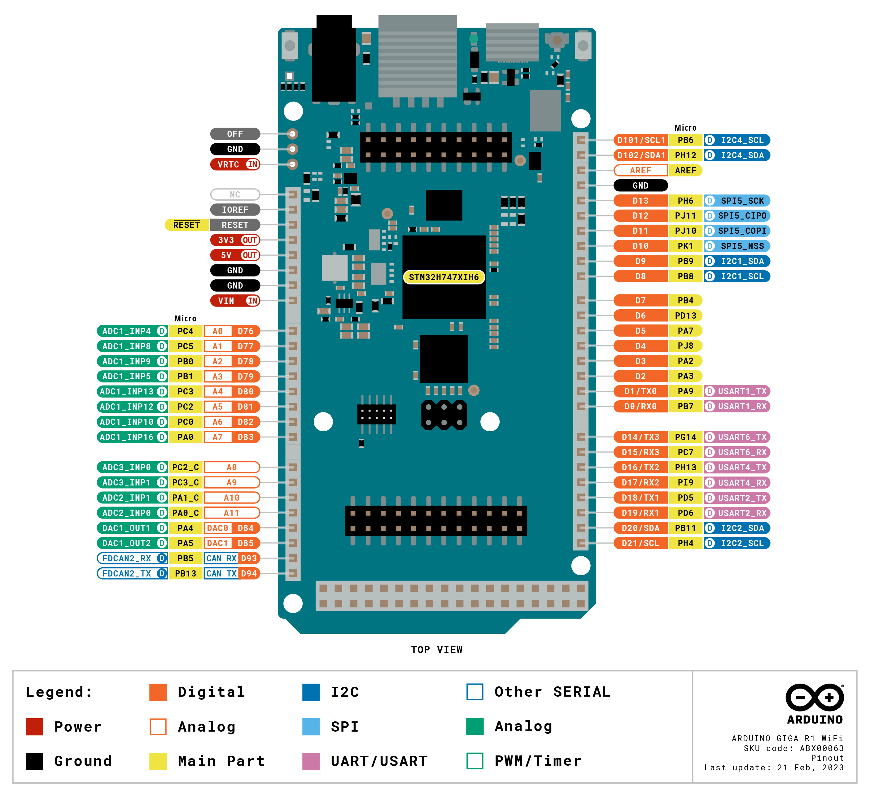
Pin reference
The Arduino Mega‑style headers expose 76 digital pins
(D0–D75), 12 analog pins (A0–A11), two DAC outputs
(DAC0/DAC1), a secondary I²C pair (SDA1/SCL1), and
an FDCAN2 pair (CAN_RX/CAN_TX). A separate 6‑pin SPI1
header on the front of the board breaks out
CIPO/COPI/SCK (D89/D90/D91).
Pin name |
Reference |
Function |
|---|---|---|
D0 |
3.3 V |
USART1 RX (Serial1) / TIM4 CH2 |
D1 |
3.3 V |
USART1 TX (Serial1) / TIM1 CH2 |
D2 |
3.3 V |
TIM2 CH4 / TIM5 CH4 / USART2 RX |
D3 |
3.3 V |
TIM2 CH3 / TIM5 CH3 / USART2 TX |
D4 |
3.3 V |
TIM8 CH1 / UART8 TX |
D5 |
3.3 V |
TIM3 CH2 / SPI1 MOSI / SPI6 MOSI |
D6 |
3.3 V |
TIM4 CH2 |
D7 |
3.3 V |
TIM3 CH1 / SPI1 MISO / SPI3 MISO / SPI6 MISO |
D8 |
3.3 V |
TIM4 CH3 / I2C1 SCL / I2C4 SCL / UART4 RX |
D9 |
3.3 V |
TIM4 CH4 / I2C1 SDA / I2C4 SDA / UART4 TX |
D10 |
3.3 V |
TIM1 CH1 / TIM8 CH3N |
D11 |
3.3 V |
TIM8 CH2 / SPI5 MOSI |
D12 |
3.3 V |
TIM8 CH2N / SPI5 MISO |
D13 |
3.3 V |
TIM12 CH1 / SPI5 SCK |
D14 |
3.3 V |
USART6 TX (Serial2) / SPI6 MOSI |
D15 |
3.3 V |
USART6 RX (Serial2) / TIM3 CH2 / TIM8 CH2 |
D16 |
3.3 V |
UART4 TX (Serial3) / TIM8 CH1N |
D17 |
3.3 V |
UART4 RX (Serial3) |
D18 |
3.3 V |
USART2 TX (Serial4) |
D19 |
3.3 V |
USART2 RX (Serial4) / SPI3 MOSI |
D20 |
3.3 V |
I2C2 SDA / TIM2 CH4 / USART3 RX |
D21 |
3.3 V |
I2C2 SCL |
D22 |
3.3 V |
GPIO |
D23 |
3.3 V |
GPIO / SPI6 SCK |
D24 |
3.3 V |
GPIO / SPI6 MISO |
D25 |
3.3 V |
GPIO |
D26 |
3.3 V |
GPIO |
D27 |
3.3 V |
GPIO |
D28 |
3.3 V |
GPIO |
D29 |
3.3 V |
GPIO |
D30 |
3.3 V |
GPIO |
D31 |
3.3 V |
GPIO |
D32 |
3.3 V |
GPIO |
D33 |
3.3 V |
GPIO |
D34 |
3.3 V |
GPIO |
D35 |
3.3 V |
GPIO |
D36 |
3.3 V |
GPIO |
D37 |
3.3 V |
TIM8 CH2 |
D38 |
3.3 V |
TIM8 CH2N |
D39 |
3.3 V |
GPIO |
D40 |
3.3 V |
TIM15 CH2 / SPI4 MOSI |
D41 |
3.3 V |
GPIO |
D42 |
3.3 V |
GPIO |
D43 |
3.3 V |
GPIO |
D44 |
3.3 V |
GPIO |
D45 |
3.3 V |
GPIO |
D46 |
3.3 V |
TIM8 CH3N |
D47 |
3.3 V |
SPI3 MOSI |
D48 |
3.3 V |
TIM8 CH3 / SPI5 SCK |
D49 |
3.3 V |
GPIO |
D50 |
3.3 V |
GPIO |
D51 |
3.3 V |
TIM15 CH1 / SPI4 MISO |
D52 |
3.3 V |
GPIO |
D53 |
3.3 V |
GPIO |
D54 |
3.3 V |
TIM8 CH1 (camera DCMI VSYNC) |
D55 |
3.3 V |
I2C3 SDA (camera DCMI HSYNC) |
D56 |
3.3 V |
TIM3 CH1 / TIM13 CH1 (camera DCMI PXCLK) |
D57 |
3.3 V |
TIM8 CH1N / UART8 RX (camera master clock — TIM1 CH3) |
D58 |
3.3 V |
TIM8 CH3 (camera DCMI D7) |
D59 |
3.3 V |
TIM8 CH2 (camera DCMI D6) |
D60 |
3.3 V |
GPIO (camera DCMI D5) |
D61 |
3.3 V |
TIM8 CH2N / UART4 RX (camera DCMI D4) |
D62 |
3.3 V |
SPI1 SCK (camera DCMI D3) |
D63 |
3.3 V |
TIM5 CH2 / I2C4 SCL (display I²C) |
D64 |
3.3 V |
TIM5 CH1 (camera DCMI D1) |
D65 |
3.3 V |
TIM12 CH2 (camera DCMI D0) |
D66 |
3.3 V |
GPIO (camera reset — claimed when camera is active) |
D67 |
3.3 V |
GPIO (camera power‑down — claimed when camera is active) |
D68 |
3.3 V |
TIM3 CH1 / TIM8 CH1 / USART6 TX (Display Shield DSI RESET) |
D69 |
3.3 V |
TIM5 CH4 (Display Shield DSI TE) |
D70 |
3.3 V |
SPI2 SCK |
D71 |
3.3 V |
TIM8 CH4 / SPI2 MISO |
D72 |
3.3 V |
SPI2 MOSI |
D73 |
3.3 V |
ADC123 IN11 (Display Shield DFSDM mic data) |
D74 |
3.3 V |
GPIO (display backlight — claimed by the Giga Display Shield) |
D75 |
3.3 V |
SPI2 SCK (Display Shield DFSDM mic clock) |
A0 / D76 |
3.3 V |
ADC12 IN4 |
A1 / D77 |
3.3 V |
ADC12 IN8 |
A2 / D78 |
3.3 V |
ADC12 IN9 / TIM3 CH3 / TIM8 CH2N |
A3 / D79 |
3.3 V |
ADC12 IN5 / TIM3 CH4 / TIM8 CH3N |
A4 / D80 |
3.3 V |
ADC12 IN13 / SPI2 MOSI |
A5 / D81 |
3.3 V |
ADC123 IN12 / SPI2 MISO |
A6 / D82 |
3.3 V |
ADC123 IN10 |
A7 / D83 |
3.3 V |
ADC1 IN16 / TIM2 CH1 / TIM5 CH1 (audio jack mic input) |
A8 |
3.3 V |
ADC3 IN0 (analog only) |
A9 |
3.3 V |
ADC3 IN1 (analog only) |
A10 |
3.3 V |
ADC12 IN1 (analog only) |
A11 |
3.3 V |
ADC12 IN0 (analog only) |
DAC0 / A12 / D84 |
3.3 V |
DAC1 OUT1 / ADC12 IN18 (audio jack line‑out L) |
DAC1 / A13 / D85 |
3.3 V |
DAC1 OUT2 / TIM2 CH1 / SPI1 SCK / ADC12 IN19 (audio jack line‑out R) |
D89 |
3.3 V |
SPI1 MISO ( |
D90 |
3.3 V |
SPI1 MOSI ( |
D91 |
3.3 V |
SPI1 SCK ( |
CAN_RX / D93 |
3.3 V |
FDCAN2 RX / TIM3 CH2 / UART5 RX |
CAN_TX / D94 |
3.3 V |
FDCAN2 TX / SPI2 SCK / UART5 TX |
SDA1 / D102 |
3.3 V |
I2C4 SDA (display touch / camera control bus) |
SCL1 / D101 |
3.3 V |
I2C4 SCL (display touch / camera control bus) |
RESET |
3.3 V |
press the on‑board RESET button or pull to GND to reset |
LED_RED |
3.3 V |
RGB LED red channel (active low) |
LED_GREEN |
3.3 V |
RGB LED green channel (active low) |
LED_BLUE |
3.3 V |
RGB LED blue channel (active low) |
Note
A8–A11 are analog‑only pads on the STM32H747’s _C
pins — they have no GPIO function and can only be read through
the ADC.
Power pins
Mega header pins:
VIN — 6–32 V input. Powers the board through the on‑board buck regulator.
+5V — 5 V rail fed from USB via a diode or the on‑board buck regulator.
+3V3 — main 3.3 V rail.
IOREF — reflects the I/O voltage of the board (3.3 V).
AREF — analog voltage reference for the ADC pins. Defaults to 3.3 V; drive externally to use a different reference.
OFF — pull to GND to turn off the +3.3 V rail and shut the system down.
VRTC — 3.0 V coin‑cell input (3.3 V max) that keeps the on‑chip RTC running while the rest of the board is powered off.
GND — common ground.
The Giga R1 can be powered through any of these paths:
USB‑C — supplies 5 V to the on‑board buck regulator.
VIN pin — drive a regulated 6–32 V supply directly.
Tip
Use the battery life estimator to model how long the Giga R1 will run on a battery for a given active / deep-sleep duty cycle.
Recovery and debug pins
RESET — both an exposed pin on the power header and a momentary switch on the top of the board, tied to the SoC’s NRST line. Pull to GND or press the button to reset.
The Giga R1 uses Arduino’s standard double‑tap reset to enter Arduino’s bootloader. Quickly press the RESET button twice — the board re‑enumerates over USB as a DFU device and OpenMV IDE can flash a new firmware image.
If the bootloader is missing entirely, hold the BOOT0 button while pressing RESET to force the SoC into ROM bootloader mode.
The STM32 SWD signals are exposed on the 10‑pin 1.27 mm Cortex Debug header on the front of the board. Wire them up via a SEGGER J‑Link, ST‑Link, or any standard ARM JTAG/SWD probe. All debug signals are 3.3 V referenced.
Onboard peripherals
LEDs
The Giga R1 has a single user RGB LED, software‑controllable through machine.LED:
from machine import LED

LED("LED_RED").on()
LED("LED_GREEN").on()
LED("LED_BLUE").on()
A separate power LED on the board lights whenever the +3.3 V rail is up and is not user‑controllable.
Camera connector (J6)
J6 is a 22‑pin Arducam‑compatible camera flex connector. Plug
in any of the supported sensor modules and the firmware probes
them automatically through the csi — camera sensors module:
import csi

cam = csi.CSI()
cam.reset()
cam.pixformat(csi.RGB565)
cam.framesize(csi.QVGA)
cam.snapshot(time=2000)       # let auto‑exposure settle

while True:
    img = cam.snapshot()
Supported sensors:
OV5640 — 5 MP colour, up to QSXGA (2592 × 1944).
OV7670 — 0.3 MP colour, up to VGA (640 × 480).
GC2145 — 2 MP colour, up to UXGA (1600 × 1200).
HM01B0 — 320 × 320 monochrome.
HM0360 — VGA (640 × 480) monochrome.
Warning
While the camera is initialised, the following Mega header pins are claimed by the firmware and cannot be used:
Pin |
Reason |
|---|---|
|
DCMI data + sync signals on the camera flex connector |
|
TIM1 CH3 — camera master clock |
|
Camera reset GPIO |
|
Camera power‑down GPIO |
|
I²C 4 — shared with the camera; bus is usable but avoid the sensor’s I²C address |
Machine learning
ml — Machine Learning runs quantised TFLite models on the Cortex‑M7
with CMSIS‑NN kernels — fast enough for compact detectors at a
few frames per second. Models on the read‑only /rom filesystem
load directly from flash without copying to RAM. Here’s a 128×128
BlazeFace detector overlaying the detected face and its six landmarks
on every frame:
import csi
import time
import ml
from ml.postprocessing.mediapipe import BlazeFace

# Initialize the sensor.
csi0 = csi.CSI()
csi0.reset()
csi0.pixformat(csi.RGB565)
csi0.framesize(csi.VGA)
csi0.window((400, 400))

# Load built-in face detection model
model = ml.Model("/rom/blazeface_front_128.tflite", postprocess=BlazeFace(threshold=0.4))
print(model)

clock = time.clock()
while True:
    clock.tick()
    img = csi0.snapshot()

    for r, score, keypoints in model.predict([img]):
        ml.utils.draw_predictions(img, [r], ("face",), ((0, 0, 255),), format=None)
        ml.utils.draw_keypoints(img, keypoints, color=(255, 0, 0))

    print(clock.fps(), "fps")
M4 core
The Cortex‑M4 core is exposed through openamp
for inter‑processor communication. The OpenMV firmware runs on the
M7 only; the M4 has no MicroPython runtime of its own, so using it
means building a separate C firmware image and loading it from the
filesystem via openamp.RemoteProc.
Pre‑built example firmware that implements a virtual UART endpoint
is available in the
openamp_vuart
repository — follow its README to build vuart.elf:
import openamp
import time

def ept_recv_callback(src_addr, data):
    print("Received:", data.decode())

ept = openamp.Endpoint("vuart-channel", callback=ept_recv_callback)

rproc = openamp.RemoteProc("vuart.elf")
rproc.start()

count = 0
while True:
    if ept.is_ready():
        ept.send("Hello World %d!" % count, timeout=1000)
        count += 1
    time.sleep_ms(1000)
In practice this support is best treated as a demonstration of the openamp interface rather than a working dual‑core platform — the M4 cannot be reset independently of the M7, so stopping the M4 forces a full system reboot.
Display (J5)
J5 is a MIPI‑DSI connector for the Arduino Giga Display
Shield — a 480 × 800 capacitive touch panel built around the
ST7701 panel driver and the GT911 touch controller. Both drivers
ship frozen with the firmware. Use display — display driver to
push framebuffers and gt911.GT911 for touch input.
The example below mirrors the camera into a portrait 800 × 480 display window and overlays each touch contact as a coloured circle:
import csi
import time
import image
import display
from gt911 import GT911
from machine import I2C

IMG_OFFSET = 80
touch_detected = False
points_colors = ((255, 0, 0), (0, 255, 0), (0, 0, 255),
                 (0, 255, 255), (255, 255, 0))

csi0 = csi.CSI()
csi0.reset()
csi0.pixformat(csi.RGB565)
csi0.framesize(csi.VGA)

lcd = display.DSIDisplay(
    framesize=display.FWVGA,
    portrait=True,
    refresh=60,
    controller=display.ST7701(),
)

# Pass pin names (not Pin objects) so the driver can flip
# the reset pin's direction during start-up.
touch = GT911(
    I2C(4, freq=400_000),
    reset_pin="D71",
    irq_pin="D70",
    touch_points=5,
    refresh_rate=240,
    reverse_x=True,
    touch_callback=lambda pin: globals().update(touch_detected=True),
)

clock = time.clock()
while True:
    clock.tick()
    img = csi0.snapshot()

    if touch_detected:
        n, points = touch.read_points()
        for i in range(n):
            img.draw_circle(
                (points[i][0] - IMG_OFFSET,
                 points[i][1],
                 points[i][2] * 3),
                color=points_colors[points[i][3]],
                thickness=2,
            )
        touch_detected = False

    lcd.write(img, y=IMG_OFFSET, hint=image.TRANSPOSE | image.VFLIP)
    print(clock.fps())
Warning
The Giga Display Shield uses the same I²C 4 bus
(SDA1/SCL1) as the camera, D74 for the LCD backlight
enable, D70/D71 for the GT911 touch IRQ and reset, and
D68/D69 for the DSI panel’s TE and RESET signals.
Microphone (Display Shield)
The Arduino Giga Display Shield carries a digital microphone wired
to the STM32H747’s DFSDM peripheral (mic clock on D75, mic data
on D73). The microphone is captured through
audio — Audio Module. Each buffer arrives as signed‑16‑bit
PCM bytearray, ready to feed into
ulab/numpy for DSP:
import audio
from ulab import numpy as np

def loudness(pcmbuf):
    samples = np.array(np.frombuffer(pcmbuf, dtype=np.int16), dtype=np.float)
    rms = np.sqrt(np.mean(samples ** 2))
    if rms > 10000:
        print("Loud!", int(rms))

audio.init(channels=1, frequency=16000, gain_db=24)
audio.start_streaming(loudness)

while True:
    pass
IMU (Display Shield)
The Arduino Giga Display Shield carries a Bosch BMI270 6‑axis
IMU (3D accelerometer + 3D gyroscope) on the same I²C 4 bus at
address 0x68. Use the community
micropython_bmi270
driver to read it:
import time
from machine import I2C
from micropython_bmi270 import bmi270

sensor = bmi270.BMI270(I2C(4, freq=400_000))
sensor.load_config_file()

while True:
    ax, ay, az = sensor.acceleration   # m/s²
    gx, gy, gz = sensor.gyro
    print(ax, ay, az, gx, gy, gz)
    time.sleep_ms(100)
The full register map is in the BMI270 datasheet.
RGB LED (Display Shield)
The Arduino Giga Display Shield carries an on‑board RGB LED driven
by an ISSI IS31FL3197 3‑channel LED driver on the same I²C 4
bus. The driver’s AD pin is tied to GND, so it sits at I²C
address 0x50. Use the community
IS31FL3197 driver to
control the LED:
from machine import I2C
from is31fl3197 import IS31FL3197

led = IS31FL3197(I2C(4, freq=400_000))
led.set_color(255, 0, 0)   # full red
The full register map is in the IS31FL3197 datasheet.
Wi‑Fi
The on‑board Murata 1DX (CYW4343W) is exposed via network — network configuration as a station interface. Connect the supplied antenna to the on‑board U.FL connector before bringing up the radio:
import network, time

wlan = network.WLAN(network.STA_IF)
wlan.active(True)
wlan.connect("ssid", "password")
while not wlan.isconnected():
    time.sleep(1)
print("Wi‑Fi IP:", wlan.ipconfig("addr4")[0])
Bluetooth
The same Murata 1DX also exposes Bluetooth LE 5.1. Use aioble — Async BLE for asyncio‑friendly BLE — for example, advertise as a peripheral and wait for a central to connect:
import asyncio
import aioble

async def run():
    while True:
        conn = await aioble.advertise(250_000, name="Giga-R1")
        print("Connected:", conn.device)
        await conn.disconnected()

asyncio.run(run())
Bus reference
GPIO
Use machine.Pin to read or drive any of the silkscreened pins. Outputs are 3.3 V CMOS and can sink/source up to 20 mA per pin (140 mA total across the whole header).
from machine import Pin

out = Pin("D2", Pin.OUT)
out.on()
out.off()
out.value(1)

inp = Pin("D3", Pin.IN, Pin.PULL_UP)
print(inp.value())
Any input pin can also fire an interrupt on edge transitions:
def handler(pin):
    print("triggered:", pin)

Pin("D3", Pin.IN, Pin.PULL_UP).irq(
    handler, Pin.IRQ_FALLING | Pin.IRQ_RISING,
)
UART
Bus |
TX |
RX |
Arduino name |
|---|---|---|---|
UART1 |
D1 |
D0 |
Serial1 |
UART6 |
D14 |
D15 |
Serial2 |
UART4 |
D16 |
D17 |
Serial3 |
UART2 |
D18 |
D19 |
Serial4 |
from machine import UART

uart = UART(1, baudrate=115200)
uart.write("hello")
uart.read(5)
I²C
Bus |
SCL |
SDA |
|---|---|---|
I2C2 |
D21 |
D20 |
I2C1 |
D8 |
D9 |
I2C4 |
SCL1 |
SDA1 |
from machine import I2C

i2c = I2C(2, freq=400_000)
i2c.scan()
i2c.writeto(0x76, b"hi")
Bus 2 (D20/D21, the silkscreened SCL/SDA) is the
default Arduino Wire bus. Bus 4 (SCL1/SDA1) is shared
with the camera and the Giga Display Shield’s GT911 touch
controller — user devices on this bus must avoid the following
addresses (7‑bit):
0x3C— OV5640 / GC21450x24— HM01B0 / HM03600x21— OV76700x5D— GT911 touch controller (Giga Display Shield)
The same hardware can also be used in target (slave) mode through machine.I2CTarget to expose a memory region to another I²C controller:
from machine import I2CTarget

buf = bytearray(32)
target = I2CTarget(2, addr=0x42, mem=buf)
SPI
Bus |
MOSI |
MISO |
SCK |
|---|---|---|---|
SPI1 |
D90 |
D89 |
D91 |
SPI5 |
D11 |
D12 |
D13 |
SPI1 is exposed on a dedicated 6‑pin header on the front of the
board. SPI5 is exposed on the silkscreened
COPI/CIPO/SCK labels on D11/D12/D13.
Note
Pinout of the front 6‑pin SPI1 header (J7):
Pin |
Signal |
|---|---|
1 |
|
2 |
+5V |
3 |
|
4 |
|
5 |
NRST |
6 |
GND |
from machine import SPI
from machine import Pin

spi = SPI(5, baudrate=10_000_000)
cs = Pin("D10", Pin.OUT, value=1)   # CS is not driven by the SPI peripheral

cs.value(0)
spi.write(b"hello")
cs.value(1)
CAN (FDCAN)
Bus |
TX |
RX |
|---|---|---|
FDCAN2 |
D94 |
D93 |
from machine import CAN

can = CAN(2, 500_000)
can.set_filters(None)
can.send(0x123, b"\xDE\xAD\xBE\xEF")
print(can.recv())
ADC
The Giga R1 exposes twelve 12‑bit ADC channels on A0–A11, all
3.3 V referenced — read_u16 returns 0–65535 across 0–3.3 V
at the pin. A8–A11 are analog‑only _C pads with no GPIO
peripheral:
from machine import ADC
import time

adc = ADC("A0")
while True:
    voltage = adc.read_u16() * 3.3 / 65535
    print(voltage)
    time.sleep_ms(100)
Note
A7 is also wired to the microphone input on the 3.5 mm
TRRS audio jack — when a headset is plugged in, ADC("A7")
reads the analog mic signal directly.
DAC
Two 12‑bit DAC channels are exposed on DAC0 and DAC1 through
pyb.DAC. Both are wired to the 3.5 mm TRRS audio jack as
the left and right line‑out channels:
from pyb import DAC

left  = DAC("DAC0")
right = DAC("DAC1")

left.write(int(0.5 * 255))    # 8‑bit, ~1.65 V
right.write(int(0.5 * 255))
PWM
Pin |
Timer / channel |
|---|---|
D0 |
TIM4 CH2 / TIM17 CH1N |
D1 |
TIM1 CH2 |
D2 |
TIM2 CH4 / TIM5 CH4 / TIM15 CH2 |
D3 |
TIM2 CH3 / TIM5 CH3 / TIM15 CH1 |
D4 |
TIM1 CH3N / TIM8 CH1 |
D5 |
TIM1 CH1N / TIM3 CH2 / TIM8 CH1N / TIM14 CH1 |
D6 |
TIM4 CH2 |
D7 |
TIM3 CH1 |
D8 |
TIM4 CH3 / TIM16 CH1 |
D9 |
TIM4 CH4 / TIM17 CH1 |
D10 |
TIM1 CH1 / TIM8 CH3N |
D11 |
TIM1 CH2N / TIM8 CH2 |
D12 |
TIM1 CH2 / TIM8 CH2N |
D13 |
TIM12 CH1 |
D15 |
TIM3 CH2 / TIM8 CH2 |
D16 |
TIM8 CH1N |
D20 |
TIM2 CH4 |
D37 |
TIM8 CH2 |
D38 |
TIM8 CH2N |
D40 |
TIM15 CH2 |
D46 |
TIM8 CH3N |
D48 |
TIM1 CH1N / TIM8 CH3 |
D51 |
TIM15 CH1 |
D54 |
TIM8 CH1 |
D56 |
TIM3 CH1 / TIM13 CH1 |
D57 |
TIM1 CH3 / TIM8 CH1N |
D58 |
TIM8 CH3 |
D59 |
TIM8 CH2 |
D61 |
TIM8 CH2N |
D63 |
TIM5 CH2 |
D64 |
TIM5 CH1 |
D65 |
TIM12 CH2 |
D68 |
TIM3 CH1 / TIM8 CH1 |
D69 |
TIM5 CH4 |
D71 |
TIM8 CH4 |
D78 / A2 |
TIM1 CH2N / TIM3 CH3 / TIM8 CH2N |
D79 / A3 |
TIM1 CH3N / TIM3 CH4 / TIM8 CH3N |
D83 / A7 |
TIM2 CH1 / TIM5 CH1 |
D85 / A13 |
TIM2 CH1 / TIM8 CH1N |
Drive any of them via machine.PWM:
from machine import Pin, PWM

pwm = PWM(Pin("D2"), freq=1_000, duty_u16=32768)
Warning
TIM1 is reserved for the camera master clock when the
camera is initialised through csi — camera sensors. Pins whose
only PWM function is on TIM1 — D1, D10, D11, D12
— cannot be PWM‑driven while the camera is active. The other
listed pins all have non‑TIM1 alternates.
Note
Several pins share timer channels:
TIM2 CH4 is on
D2andD20.TIM2 CH1 is on
D83/A7andD85/A13.TIM3 CH1 is on
D7,D56, andD68.TIM3 CH2 is on
D5andD15.TIM4 CH2 is on
D0andD6.TIM5 CH1 is on
D64andD83/A7.TIM5 CH4 is on
D2andD69.TIM8 CH1 is on
D4,D54, andD68.TIM8 CH1N is on
D5,D16,D57, andD85/A13.TIM8 CH2 is on
D11,D15,D37, andD59.TIM8 CH2N is on
D12,D38,D61, andD78/A2.TIM8 CH3 is on
D48andD58.TIM8 CH3N is on
D10,D46, andD79/A3.TIM15 CH1 is on
D3andD51.TIM15 CH2 is on
D2andD40.
Pick one consumer per timer channel.
Software bit‑banged buses
machine.SoftI2C and machine.SoftSPI work on any GPIO if you need an extra bus.
Thermal sensor (off‑board)
The firmware includes the fir — thermal sensor driver (fir == far infrared) driver for externally wired thermal imagers:
MLX90621 — 16 × 4 IR array
MLX90640 — 32 × 24 IR array
MLX90641 — 16 × 12 IR array
AMG8833 — 8 × 8 IR array
Wire the module to the board’s I²C bus and read frames with
fir.init() + fir.snapshot():
import time
import image
import fir

fir.init()                          # auto‑detects the sensor
clock = time.clock()

while True:
    clock.tick()
    try:
        img = fir.snapshot(x_scale=5, y_scale=5,
                           color_palette=image.PALETTE_IRONBOW,
                           hint=image.BICUBIC,
                           copy_to_fb=True)
    except OSError:
        continue
    print(clock.fps())
The fir driver only talks to the sensor over I²C 1 — wire
the module to D8 (SCL) and D9 (SDA).
Timing
time
The time module covers blocking delays, monotonic ticks, and
elapsed‑time measurement:
import time

time.sleep(1)              # seconds
time.sleep_ms(500)
time.sleep_us(10)

start = time.ticks_ms()
# ...do work...
elapsed = time.ticks_diff(time.ticks_ms(), start)
Virtual timers
machine.Timer schedules periodic or one‑shot
callbacks without consuming a hardware timer slot. Pass -1 as
the id to use a virtual (software) timer:
from machine import Timer

one_shot = Timer(-1)
one_shot.init(period=5_000, mode=Timer.ONE_SHOT,
              callback=lambda t: print("once"))

periodic = Timer(-1)
periodic.init(period=2_000, mode=Timer.PERIODIC,
              callback=lambda t: print("tick"))
Period values are in milliseconds. Call deinit()
to stop and release the slot.
Real‑time clock
machine.RTC keeps wall‑clock time across
resets — and across full power‑off when a coin cell is connected to
the VRTC pin:
from machine import RTC

rtc = RTC()
rtc.datetime((2026, 4, 30, 4, 12, 0, 0, 0))   # Y, M, D, weekday, h, m, s, subsec
print(rtc.datetime())
Watchdog
machine.WDT resets the board if the application hangs. Once started it can’t be stopped or reconfigured — feed it periodically inside your main loop:
from machine import WDT

wdt = WDT(timeout=5_000)   # 5 second window
while True:
    # ...do work...
    wdt.feed()
Boot and runtime info
Firmware update (DFU)
The Giga R1 uses Arduino’s standard double‑tap reset to enter Arduino’s bootloader. Quickly press the RESET button twice — the board re‑enumerates over USB as a DFU device and OpenMV IDE can flash a new firmware image. If the bootloader is missing entirely, hold the BOOT0 button while pressing RESET to force the SoC into ROM bootloader mode.
A running script can re‑enter the bootloader on demand by calling
machine.bootloader():
import machine

machine.bootloader()
Filesystem and boot order
The Giga R1 firmware mounts up to two filesystems on boot:
Internal flash — always mounted at
/flash. Holdsmain.pyandREADME.txtby default; created on the very first boot.ROMFS — read‑only, memory‑mapped filesystem at
/rommounted automatically by MicroPython at startup.
After mounting, the working directory is set to /flash. The
interpreter then runs scripts from that directory:
boot.pyis executed on every soft reset (cold boot,Ctrl‑Dfrom the REPL, or whenever the running script returns).main.pyis executed only on cold boot, immediately afterboot.py. Subsequent soft resets re‑runboot.pybut drop straight to the REPL — to re‑runmain.pyyou have to fully reset the board.
The default main.py shipped on a freshly flashed board just
blinks the user RGB LED’s blue channel as a heartbeat (two short
pulses, short gap), so you can tell the firmware booted cleanly
without any host attached.
sys.path is extended to include both filesystems and their
lib/ subdirectories, so importable modules can live in
/flash/lib or /rom/lib.
When connected over USB, /flash also enumerates as a USB
mass‑storage drive on the host, letting you edit boot.py,
main.py, and any other files directly. Eject the drive before
resetting the board so the host flushes its cached writes.
Note
Because the OS treats the drive as a passive block device, files created or modified by code running on the camera will not show up until the host re‑mounts the drive. If both the OS and the camera write the same filesystem at the same time, the OS will win and overwrite changes made by the camera.
Note
The user RGB LED’s red channel may briefly light up while the host is reading from or writing to the USB mass‑storage drive — this is a firmware‑driven activity indicator, not a fault.
Storage sizes
The Giga R1 ships with:
/flash— 11 MB FAT filesystem, read/write./rom— 4 MB read-only memory-mapped ROMFS, used to ship scripts and ML models that benefit from zero-copy mmap access.
Hard‑fault indicator
If the user RGB LED is rapidly cycling through all colours — fast enough that it tends to look like a twinkling white LED rather than distinct hues — the firmware has hit an unrecoverable hard fault. Reflash the firmware to recover; if reflashing doesn’t help, the board may be physically damaged.
Software libraries
See the library index for the full list of modules — including which ones are unique to the Giga R1 build.